15 years one-stop China custom CNC machining parts factory

Hey there I’m VMT Sam!
With 25 years of CNC machining experience we are committed to helping clients overcome 10000 complex part-processing challenges all to contribute to a better life through intelligent manufacturing. Contact us now
 0 |
Published by VMT at Jun 18 2026 | Reading Time:About 3 minutes
0 |
Published by VMT at Jun 18 2026 | Reading Time:About 3 minutes


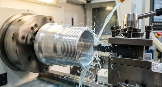
The semiconductor equipment market is riding a surge in AI accelerator chips, 5G infrastructure, and high-performance computing (HPC). If you are working around the clock to bring the next generation of lithography, etching, and thin-film deposition tools to market — quickly and without quality compromises — you need to understand one thing first: precision machining of the parts that go inside these tools.
Semiconductor CNC machining demands micron-level tolerances, contamination control, and outgassing discipline. Materials like 6061 aluminum, 316L stainless steel, and PEK require cleanroom-grade process flow that ordinary machine shops cannot match.
Inside semiconductor equipment — whether you are looking at a gas distribution plate, a vacuum chamber, or a wafer carrier — manufacturing standards are exacting. Sub-surface damage control, outgassing treatment, and cleanroom packaging are requirements that ordinary machining methods and ordinary production management cannot satisfy.
This article walks through the most common parts you will encounter in semiconductor CNC machining, the materials you can specify with confidence, the design traps to avoid, and what drives cost and lead time. At the end, we share a case study on solving a manufacturing challenge for a stainless-steel gas distribution plate.
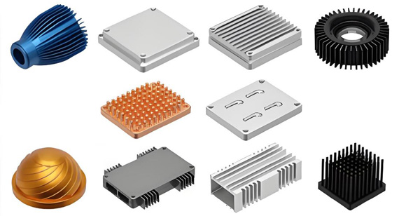
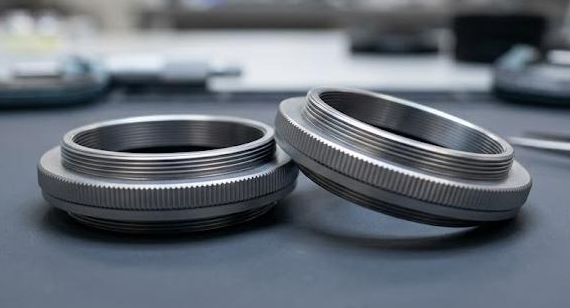
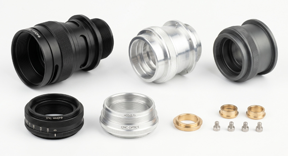
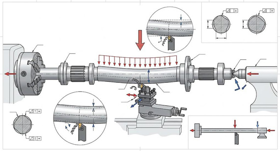
If you are scoping a new semiconductor parts project, the categories below are the ones you will encounter most often. Each one has a defined application and a fixed precision envelope.
1.CNC Semiconductor Gas Distribution Plates (GDPs)

2.CNC Semiconductor Vacuum Chambers

3.CNC Semiconductor Wafer Carriers / Pedestals / Chuck Bases

4.CNC Semiconductor Showerheads

5.CNC Semiconductor End Effectors

6.CNC Semiconductor Valve Parts

Material selection for semiconductor parts directly determines whether downstream machining is controllable, whether surface treatment can meet fab standards, and what the outgassing and contamination profile will look like at shipment.
The table below is the working BOM VMT has converged on over years of semiconductor work. Use it as your starting point during design.
| Material |
Typical Grades |
Key Characteristics |
Typical Semiconductor Use |
| Aluminum alloys |
6061, 7075 | Easy to machine, anodizable, controlled outgassing | Chamber liners, carrier bases, gas lines |
| Stainless steel |
316L (low sulfur), 304L | Corrosion-resistant, electropolishable, weldable | GDPs, valves, welded gas channels |
| Precipitation-hardened stainless |
17-4 PH (H900 / H1025) | High strength, electropolishable, outgassing-controllable | High-strength carriers, positioning blocks |
| Engineering plastic (vacuum grade) |
PEEK (VICTREX 450G vacuum grade), Vespel | Low outgassing, plasma-resistant, precision-turnable | End effectors, insulating spacers, seal supports |
| Engineering plastic (general) |
PTFE, general-grade PEEK | Chemically stable, easy to machine | Non-vacuum seals and gaskets |
Three Hidden Constraints When You Select Materials
Surface treatment is actually defines whether the part can go on the tool. Semiconductor fabs set hard requirements on surface finish, outgassing rate, and particle shedding, and any one of those failing forces the whole batch back for rework.
The table below lists most common used surface treatments for semiconductor parts and where each one fits.
| Treatment |
Typical Process Parameters |
Typical Application |
Please be Aware of... |
| Type II anodize (sulfuric) |
Film 5–25 µm, mild Ra impact | Aluminum chamber liners, carriers, panels | Film uniformity, seal quality, no visible defects |
| Type III hardcoat anodize |
Film 25–75 µm, high hardness | Plasma-facing surfaces and high-wear regions | Film uniformity, breakdown voltage, Ra delta |
| Electropolish |
20–40 µm material removal, Ra(suface roughness) drops sharply | Stainless GDPs, valves, welded gas channels | Final Ra, sub-surface damage layer removed |
| Passivation (per ASTM A967) |
Nitric or citric passivation | Post-weld stainless treatment | No free iron, complete passive film |
Two Common Misconceptions About Surface Treatment
Tolerance on semiconductor parts should work together with cleanliness, surface treatment, and outgassing control as one coherent capability system. The table below is the baseline on semiconductor work.
| Capability Dimension |
Capability Requirement |
Typical Application |
| Dimensional tolerance |
±0.005 mm typical | Critical locating faces, seal surfaces |
| Geometric tolerance |
Flatness ≤ 0.01 mm; roundness ≤ 0.005 mm | Valve seats, carrier faces |
| Surface roughness |
Ra ≤ 0.4 µm (post-electropolish) | Process-gas-wetted surfaces |
| Hole position |
±0.02 mm (5-axis single-setup) | Showerheads, gas channels |
| In-process inspection |
On-machine CMM + offline CMM | 100% of critical dimensions |
| Process capability |
Cpk ≥ 1.67 (critical features) | Volume-production critical steps |
| Temperature control |
Machining cell ±1°C | Micron-precision parts |
Three Questions You Should Put to Your Supplier
What semiconductor parts really demand is consistency — same drawing, same material lot, two adjacent machines, parts that still interchange. This means the shop has to operate as a closed loop across five dimensions: people, equipment, material, method, and environment. As you evaluate a supplier, run through these five dimensions one by one.
First, people. Machining and inspection of semiconductor parts must be done by trained, certified operators, and inspectors must be able to read the GD&T that defines critical features.
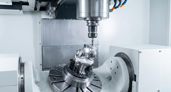
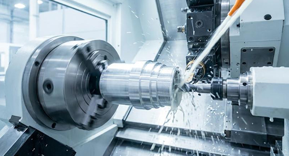
Second, equipment. A 5-axis machining center (such as a Hermle C 250 U), in-process measurement, and a temperature-stable machining environment are the foundation of micron-level precision. If a supplier's setup is a 3-axis machine with a trunnion, complex surfaces and deep cavities can only be done through multi-setup error stacking.
Third, material. Every incoming lot needs a Mill Certificate, heat number, and chemical composition report. And materials with special outgassing requirements — vacuum-grade plastic, extra-low-carbon stainless — must be stored and labeled separately.
Fourth, method. Every part family should have a Standard Operating Procedure (SOP), a tool list, a cutting-parameter table, and an inspection plan.
Fifth, environment. Cleaning, assembly, and packaging of semiconductor parts must happen in a Class 100 to Class 1000 cleanroom. The cleanroom itself needs scheduled particle counts and airborne microbe testing.
When you receive a shipment, you can ask the factory for the documents below to protect quality across the whole production chain:

If you are evaluating a new machining partner, the three checks below will tell you quickly whether they have real semiconductor capability.
First, look at their floor. Is the cleanroom a real Class 100 / 1000 environment, or is it an ordinary shop with an air purifier bolted on? Do cleaning, assembly, and packaging happen end-to-end inside the controlled space? This directly drives the particle count on parts at shipment.
Second, look at their metrology. On-machine CMM, laser interferometer, profilometer, surface roughness tester — the equipment on the metrology bench sets the ceiling of what they can actually measure. If the supplier's data is calipers and micrometers only, their hard capability ceiling sits at the 0.01 mm level.
Third, look at their outgassing and contamination control experience. If the supplier has shipped production lots of vacuum-grade plastic, anodized aluminum, and electropolished stainless, their process window has been validated. The reverse case — a shop running these parts for the first time — means you should reserve extra time and budget for qualification.
Picking a supplier is therefore not about the lowest unit price. It is about whether they can deliver in-spec parts consistently.
A Tier-1 semiconductor equipment OEM was building a prototype etch tool. The internal 316L stainless-steel gas distribution plate — 84 gas ports plus internal cross-flow channels — had been rejected by two prior shops. Port position was out by 0.04 mm, port edges had burrs, and internal channel wall roughness was Ra 0.9 µm, well above the design spec.
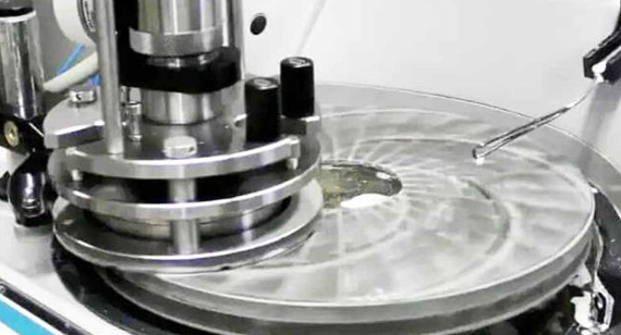
The core difficulties. Three blockers were stacked. First, the 84 ports sat on an irregular curved surface, and 3+2-positioned drilling accumulated position error far beyond tolerance. Second, 316L work-hardened severely, ordinary drills broke on the second material layer, and burr control was poor. Third, the part needed clean packaging, but the shop only had a regular production floor plus a basic clean bag.
The solution. VMT engineering reviewed the print and rebuilt the approach along three lines. First, the machining strategy was moved to 5-axis simultaneous drilling on a Hermle C 250 U 5-axis VMC inside a temperature-controlled (±1°C) cell — all 84 ports drilled in a single setup using high-precision micro drills (Ø 1.5 mm carbide, polished flutes), with in-process probing between drilling cycles to confirm hole position and diameter. Second, the internal channels were machined with custom long-reach end mills designed for the part's channel geometry, and the entire gas-wetted surface was electropolished down to a measured Ra of 0.32 µm (against a 0.4 µm spec), with 25-30 µm of material removal to eliminate sub-surface damage from machining. Third, the cleaning and packaging protocol was rewritten: multi-stage ultrasonic cleaning with deionized water, vacuum drying, a 200°C × 24-hour pre-vacuum bake cycle to reduce outgassing, and Class 100 cleanroom double-bagging with nitrogen purge.
The result. All 84 ports came in at ±0.015 mm position (against ±0.025 mm required). Internal channel wall Ra measured 0.32 µm (against Ra < 0.4 µm required). No visible burr at any port. Bake-out outgassing data: TML 0.6% and CVCM 0.04%, both better than the NASA ASTM E595 standard. The prototype tool was delivered more than 30% faster than the customer's internal target.
Succeeding at semiconductor CNC machining means controlling scrap risk on multiple fronts — ultrasonic cleaning, sub-surface damage control, rigorous inspection reporting, outgassing data. As the stainless GDP case above shows, bringing DFM review in early does more than catch machining-hardening and burr-contamination traps: it routinely cuts prototyping lead time by 30% or more while still holding micron-level precision.
If you are facing tolerance walls, hard-to-machine materials, or surface-treatment specs that fall short of fab standards, contact our senior engineering team for a free DFM and feasibility assessment with quote.

Can you machine thin-walled structures in PEEK without dimensional drifting?
Yes, but it requires patience. During PEEK machining for semiconductor isolation parts, thin walls tend to flex. We solve this by using ultra-sharp diamond-coated tools, taking light skim cuts, and using custom-milled soft jaws to support the walls, keeping tolerances within ± 0.01 mm.
How do you prevent burrs in complex internal intersections?
Internal burrs are a nightmare for wafer yield. For complex gas manifold CNC machining, we use specialized micro-tools, optimized toolpaths, and proprietary chemical or electrochemical deburring processes. This ensures every intersection within the internal gas channels is 100% burr-free and smooth.
What is the standard lead time for a semiconductor CNC machining prototype?
For standard precision semiconductor components made from aluminum or stainless steel, our typical lead time is 5 to 7 business days. If your design requires complex gas manifold CNC machining or specialized surface treatments like electropolishing, it may take 1.5 to 2 weeks. Choosing our high-precision CNC machining service ensures we optimize the workflow to meet your tight schedules.
Do you provide cleanroom packaging and ultrasonic cleaning for vacuum parts?
Yes. To ensure contamination control & cleanroom packaging standards are met, all our semiconductor components undergo multi-stage ultrasonic cleaning to remove cross-contamination, oils, and particulates. Parts are then sealed in double-layer vacuum bags within a controlled environment so they arrive ready for your cleanroom or vacuum chamber assembly.
How is semiconductor machining different from medical or aerospace machining?
Each industry has a different priority stack. Medical machining prioritizes biocompatibility, sterilization compatibility, and traceability (often under ISO 13485). Aerospace machining prioritizes strength-to-weight, fatigue life, and material certification (often under AS9100). Semiconductor machining prioritizes cleanliness, outgassing, sub-surface damage control, and micron-level tolerances.
What tolerances are required for semiconductor parts?
±0.01–0.025 mm is typical for critical features, with flatness and parallelism held to 0.01 mm or better across 200–300 mm lengths. The exact tolerance depends on the part's function — a gas port diameter might be ±0.01 mm, while a chamber body wall might be ±0.05 mm.
The technical information and manufacturing advice shared on the VMT website are for general guidance only. While we strive for accuracy, VMT does not guarantee that the processes, tolerances, or material properties mentioned are applicable to every specific project. Any reliance you place on such information is strictly at your own risk. It is the buyer's responsibility to provide definitive engineering specifications for any production orders. Final specifications and service terms shall be subject to the formal contract or quotation confirmed by both parties.

 +86 15099911516


 Read more